Modeling of pixels in CMOS sub-100nm technologies
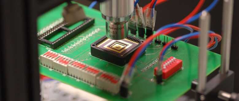
The rapid scaling of CMOS technologies and the development of optimized CIS (CMOS Image Sensor) processes for CMOS vision products has not been met by a similar effort in a comprehensive study of the main physical phenomena dominating the behavior of pixels at these technological nodes. To the best of our knowledge thorough studies exist down to 0.18µm processes but the viability of 90nm, 65nm and below implementations remains unclear. This poses severe limitations and jeopardizes the potential benefits of technology downscaling in developing innovative devices and applications that can improve the quality of services in health, safety and security, transport, and environment, just to mention a few. This project aims at tackling this shortcoming by means of the development of accurate physical models of pixels and photodiodes in advanced sub-100nm CMOS technologies. Moreover, as industrial design and mass production are only possible using CAD tools, the project contemplates the translation of this analytical model into hardware description languages such as VHDL-AMS to be used in standard CAD tools.
Objectives
- Development of accurate physical models of pixels and photodiodes in CMOS sub-100nm technologies.
- Fabrication and characterization of pixels in CMOS 65nm.
- Determination of practical scaling limits of pixels in CMOS technologies.
- Design of innovative pixel architectures.
- Translation of the pixel analytical models in hardware description languagues.
Project
/research/projects/modelado-de-pixeles-en-tecnoloxias-cmos-sub-100nm
<p>The rapid scaling of CMOS technologies and the development of optimized CIS (CMOS Image Sensor) processes for CMOS vision products has not been met by a similar effort in a comprehensive study of the main physical phenomena dominating the behavior of pixels at these technological nodes. To the best of our knowledge thorough studies exist down to 0.18µm processes but the viability of 90nm, 65nm and below implementations remains unclear. This poses severe limitations and jeopardizes the potential benefits of technology downscaling in developing innovative devices and applications that can improve the quality of services in health, safety and security, transport, and environment, just to mention a few. This project aims at tackling this shortcoming by means of the development of accurate physical models of pixels and photodiodes in advanced sub-100nm CMOS technologies. Moreover, as industrial design and mass production are only possible using CAD tools, the project contemplates the translation of this analytical model into hardware description languages such as VHDL-AMS to be used in standard CAD tools.</p><ol><li>Development of accurate physical models of pixels and photodiodes in CMOS sub-100nm technologies.</li><li>Fabrication and characterization of pixels in CMOS 65nm.</li><li>Determination of practical scaling limits of pixels in CMOS technologies.</li><li>Design of innovative pixel architectures.</li><li>Translation of the pixel analytical models in hardware description languagues.</li></ol> - Paula López Martínez - Víctor Manuel Brea Sánchez, Diego Cabello Ferrer
projects_en